ARM-Subset Multicycle CPU on FPGA
Overview
Progressive hardware design project building from foundational components up to a fully functional multicycle ARM-subset processor, synthesized and verified on an Altera DE0-Nano FPGA (Intel Cyclone IV EP4CE22F17C6). The project spans four lab stages, each adding a layer of microarchitectural complexity.
Architecture Progression
- LAB 1 — Building Blocks: Parametrized 8-operation ALU, 4-register file with dual-read/single-write ports, multiplexers and decoders used throughout the design.
- LAB 2 — Datapath + Booth’s Multiplier: Integrated datapath controlled by a finite state machine; signed multiplication via Booth’s algorithm with 2’s complement correction and shift-register accumulation.
- LAB 3 — Single-Cycle Processor: Complete single-cycle CPU supporting data-processing (ADD, SUB, AND, ORR, LSL, LSR, CMP) and memory instructions (LDR, STR). Combinational controller decodes op/function codes into control signals.
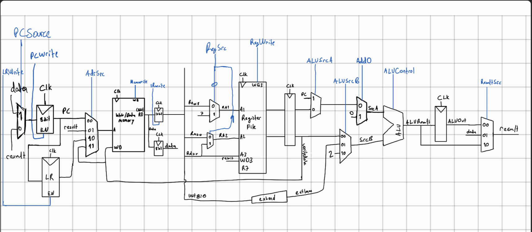
- LAB 4/5 — Multicycle Processor: Instruction execution spread across FSM states (FETCH → DECODE → EXECUTE1 → EXECUTE2/3), enabling resource sharing across stages. Adds full branching support: conditional (BEQ, BNE, BCS, BCC), indirect (BX), and link register (BL).
Datapath Diagram
Datapath Features
- 16×32-bit register file with dual read / single write ports
- 32-bit ALU with 8 operations and condition flags (carry, overflow, zero, negative)
- Barrel shifter for efficient shift operations within the ALU
- Separate synchronous instruction and data memory subsystems
- Immediate value extension and condition code evaluation
Technology Stack
- Language: Verilog (IEEE 1364)
- Target Hardware: Intel Cyclone IV EP4CE22F17C6 — Altera DE0-Nano board
- Tools: Intel Quartus Prime 20.1 Lite (synthesis), ModelSim-Altera (simulation)